Precision-Engineered PCBs: Flawless Design and Layout
for Optimal Performance
At MGX Technologies s. r. o., we transform your innovative ideas into tangible hardware through expert Printed Circuit Board (PCB) and layout design.
Our meticulous approach ensures your electronic products are not only functional and reliable but also optimized for manufacturing
and cost-efficiency.
From Concept
to Production-Ready Files
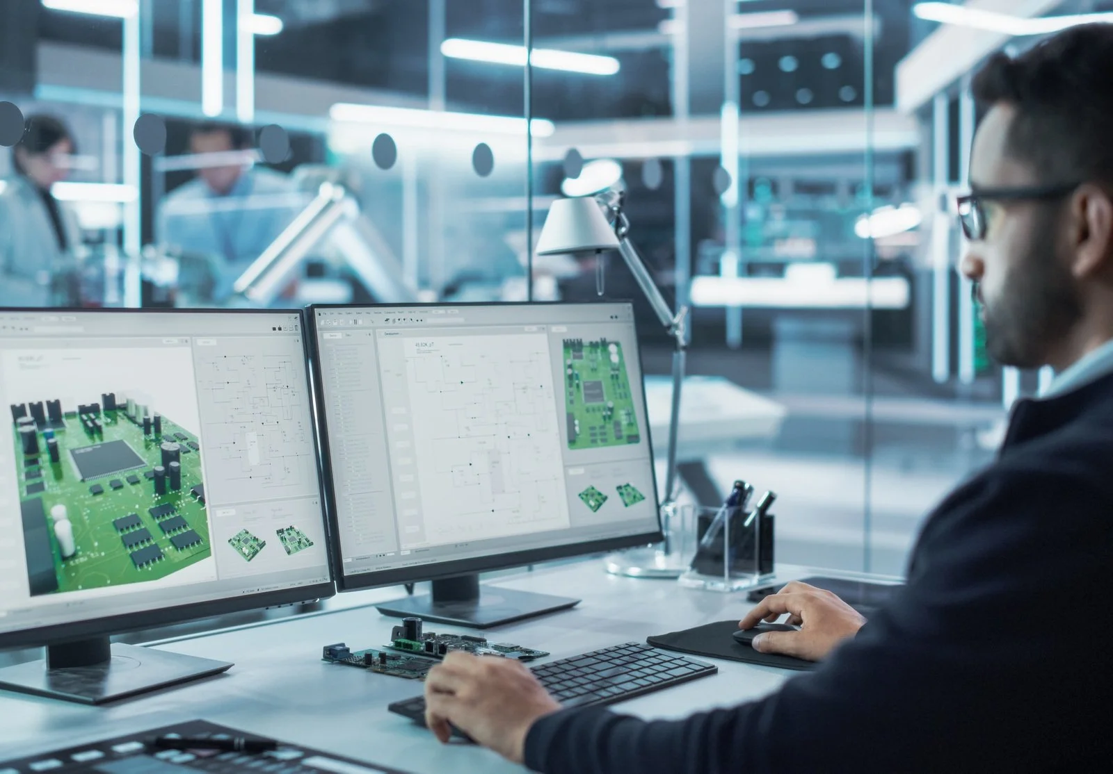
We handle the entire PCB design lifecycle, working closely with you to understand your specific requirements and performance goals.
Our designs rigorously adhere to IPC standards for the highest level of quality and reliability. Furthermore, for space-grade applications, we meticulously follow the ECSS-Q-ST-70-12C standard ("Design rules for printed circuit boards"), ensuring designs meet the stringent demands of aerospace environments.

Our PCB design and layout services include:
-
We translate your circuit concepts into detailed schematics, meticulously selecting components and defining interconnections to ensure optimal performance.
-
We create precise and accurate footprints for all components, adhering to industry standards and DFM (Design for Manufacturability) guidelines.
-
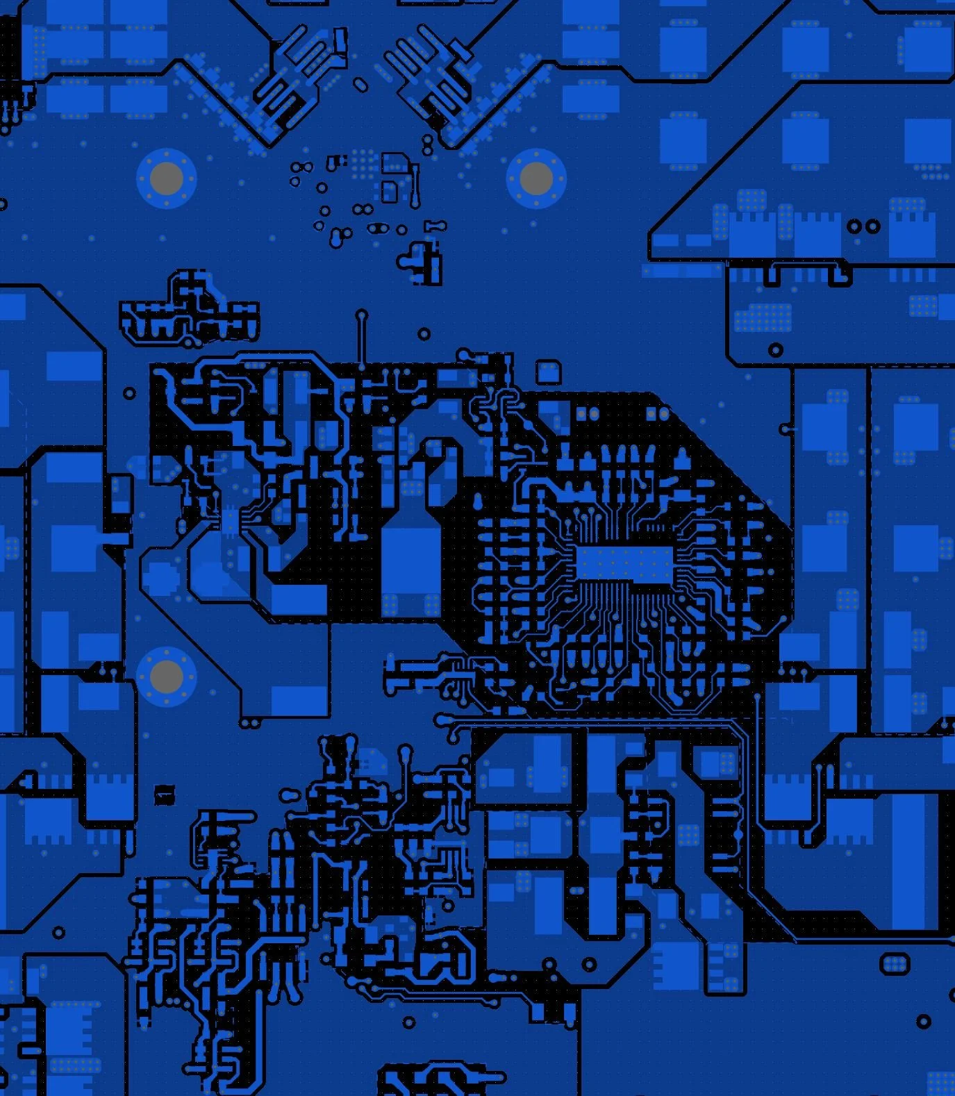
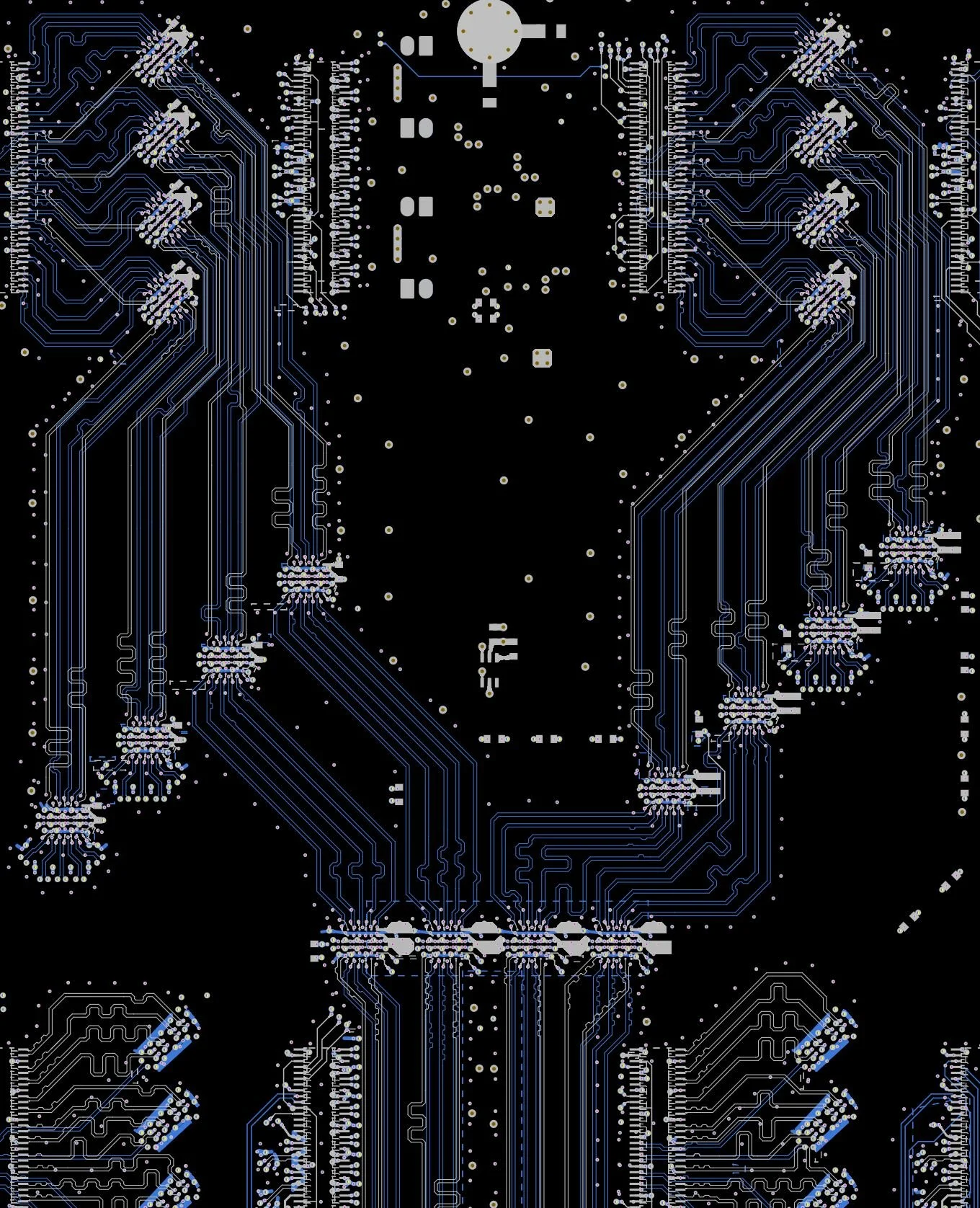
Specializing in intricate designs, we tackle challenges like high-speed routing, impedance control, signal integrity, power integrity for complex multi-layer boards, and are highly capable in High-Density Interconnect (HDI) designs for miniaturization and advanced performance.
-
Expertise in designing rigid-flex boards for compact, dynamic applications, as well as specialized PCB build-ups for extreme thermal management, including heavy copper PCBs, copper coin PCBs, and other custom solutions for high current handling and superior heat dissipation.
-
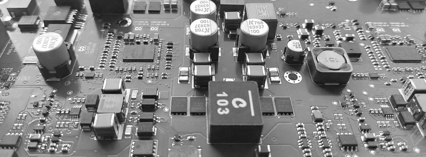
We optimize your PCB layout for efficient and cost-effective manufacturing and assembly, minimizing potential issues and rework.
-
We integrate effective thermal solutions into the layout to ensure optimal operating temperatures and extend component lifespan.
-
Our designs inherently incorporate best practices to minimize electromagnetic interference, ensuring your product meets regulatory compliance.
-
We deliver comprehensive, production-ready manufacturing files (Gerber files, drill files, BOM, pick-and-place data, Assembly instructions) and detailed documentation for seamless fabrication.
Why Choose us
for PCB & Layout Design?
Our team comprises seasoned PCB design engineers with a deep understanding of diverse industries and technologies.
Experienced Engineers
We leverage industry-leading EDA (Electronic Design Automation) tools and employ cutting-edge design methodologies.
Advanced Tools & Techniques
We prioritize robust design practices to ensure the highest levels of performance, reliability, and longevity for your products.
Quality & Reliability
Our designs are optimized to reduce manufacturing costs without compromising on quality or functionality.
Cost-Efficiency
We understand the importance of your project timelines and are committed to delivering on schedule.
Timely Delivery