How to set Design Rule in Altium Designer for all Pads Direct Connection to Polygons at specific Component
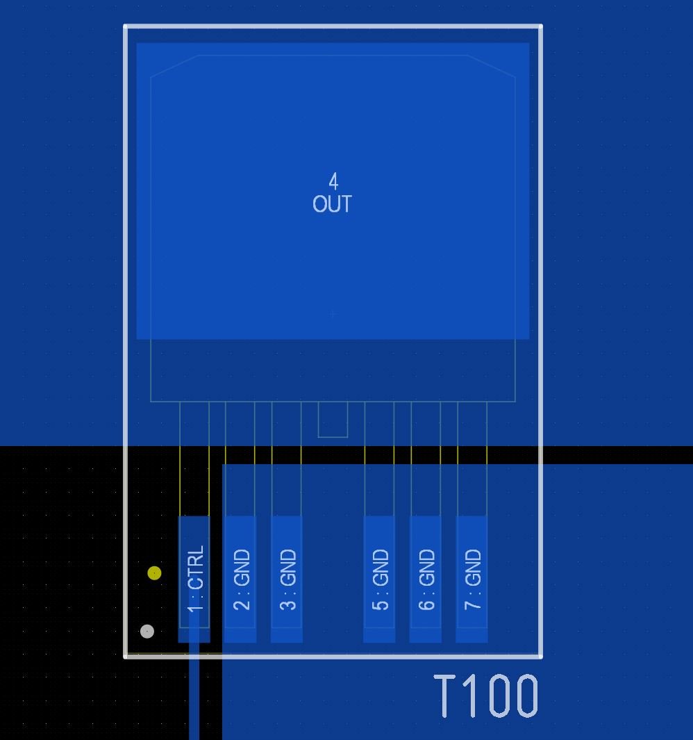
Desired settings for Altium Designer Design Rules for Direct Polygon connection for transistor T100
The challenge: Set Altium Designer Design Rules for Polygon Direct Connection for specific component(s)
Image above presents desired state of Altium Designer Design Reles setting for Direct Polygon connection at all Pads at transistor T100 (example).
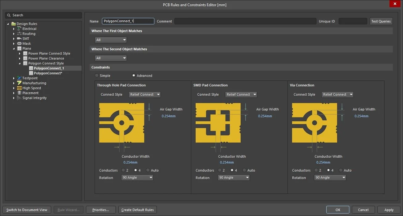
Altium Designer Default Polygon Connection
Image below presents output for default rule for Polygon connection - Relief Connect.
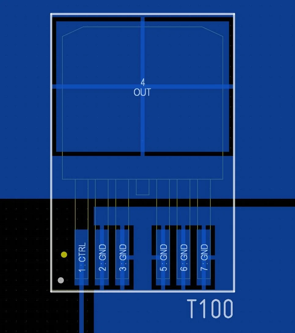
Default settings for Altium Designer Design Rules for Relief Polygon connection for all components
How set Design Rule in Altium Designer for all Pads Direct Connection to Polygons at specific Component
In Altium Designer when PcbDoc document is open, click Design >> Rules,
Popup window PCB Rules and Constraints Editor is opened:
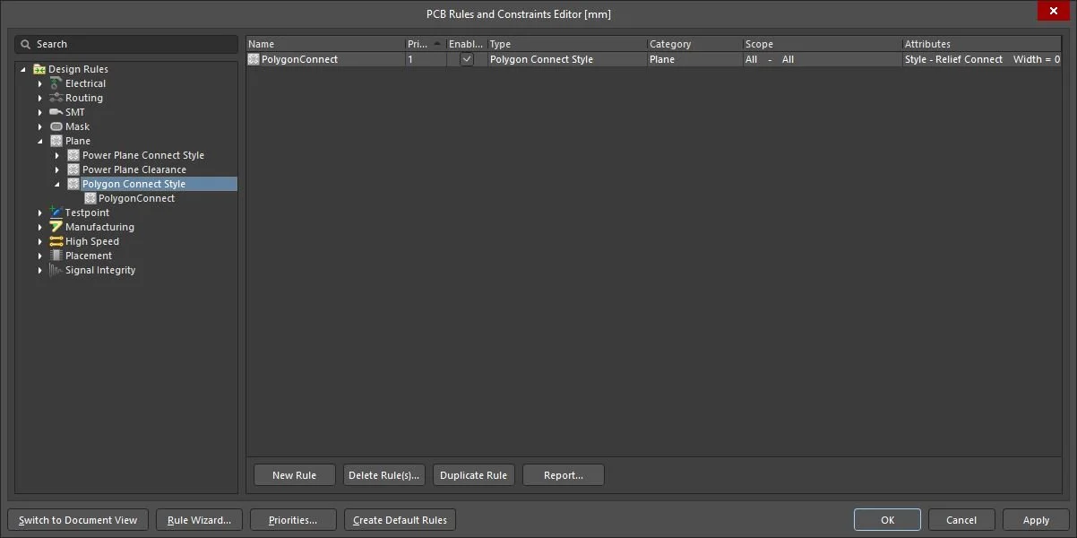
PCB Rules and Constraints Editor - Default
In Design Rules tree, locate rule Plane >> Polygon Connect Style, and right click New Rule:
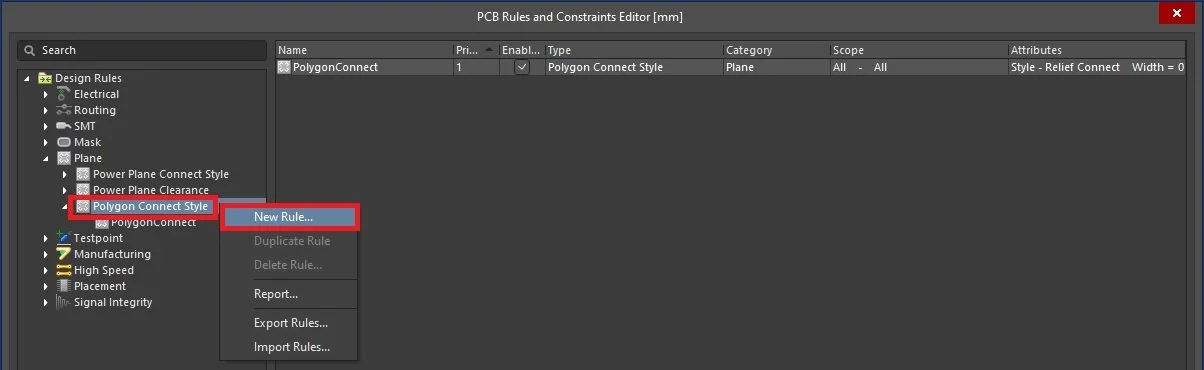
Creation of new rule for Polygon Connect Style
New empty rule is created:
Empty rule for Polygon Connect Style
In the rule editor window enter rule Name (e.g. PolygonConnect_Direct_Component), in second object matches select Custom Query and enter rule for desired component T100 selection InComponent('T100') and defined Constraints to Simple and Connect Style to Direct Connect:
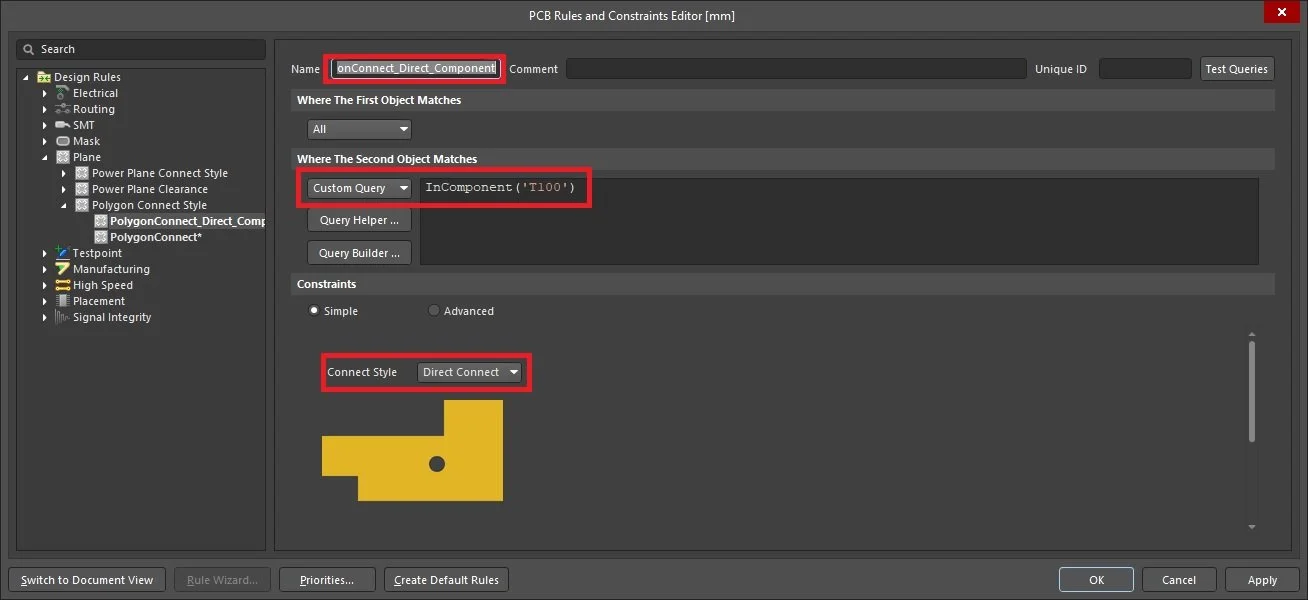
Definition of new rule for Polygon Direct Connection for specific component
Click OK button when rule is created.
Repour all polygons to get desired outcome for Polygon connection.
Adding more components for direct Polygon Connection
To add other specific component to group of direct Polygon Connections, simply add reference of component to the rule (example for T101):
InComponent('T100','T101')
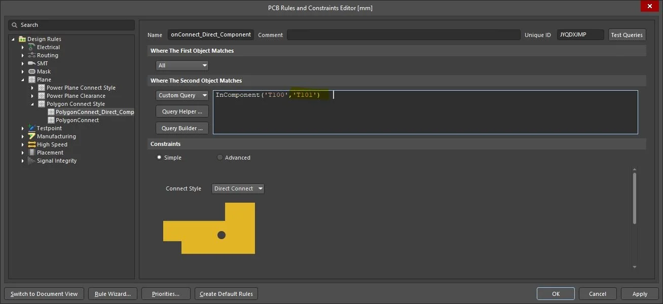
Adding next component to group of direct connected components to Polygon